


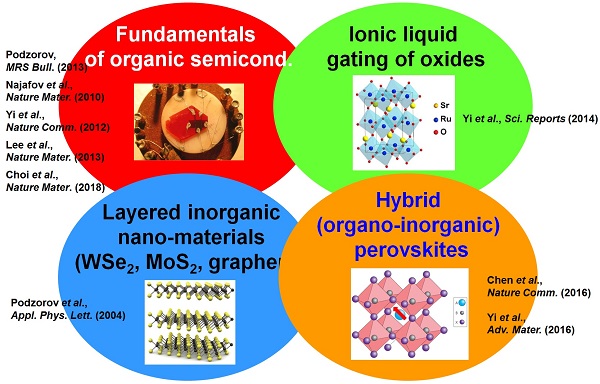
Research Themes
Organic Electronics
Organic electronics is an interdisciplinary research field focusing on organic (carbon-based) molecular semiconductors, as opposed to traditional inorganic (covalently-bonded) semiconductors, such as silicon or germanium. Organic devices include, for instance, organic field-effect transistors (OFETs), light emitting diodes (OLEDs) and organic photo-voltaic (OPV) cells. This technology is envisioned to help us addressing a number of important problems of modern society, such as renewable energy, flexible, wearable and disposable electronics, as well as sensors and actuators. It might also help overcoming the limitations of modern semiconductor nanostructures. This field may lead to technologies, such as flexible, rollable computer and TV screens, electronic paper, solar cells, energy efficient solid-state lighting, photo-detectors and chemical or biological molecular sensors. These kinds of technologies are becoming increasingly important in modern World, but yet they are difficult to tackle using conventional inorganic semiconductors. In addition, due to the vast combinatorial possibilities of synthetic chemistry and compatibility of organic semiconductors with inexpensive solution-based, printing or vacuum deposition techniques, these materials represent the technology of the future.
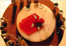
Despite the progress in applied research on organic semiconductors, a range of the fundamental aspects of organic semiconductors, including charge (polaron) and energy (exciton) generation and transport, remain poorly understood. Therefore, our interests lie in the basic physics of organic semiconductors that determine the operation of organic transistors and solar cells. With the development of single-crystal OFETs, we can study the intrinsic charge transport and optical properties of organic semiconductors, without limitations imposed by disorder present in amorphous and polycrystalline organic films (see, e.g., a review here V. Podzorov, MRS Bulletin (2013)). Owing to a great reproducibility and a very low density of defects (traps) in our single-crystalline devices, the experimental observations of a band-like polaronic transport (V. Podzorov et al., Phys. Rev. Lett. (2004)), Hall effect (V. Podzorov et al., Phys. Rev. Lett. (2005)), and novel photo-induced phenomena became possible in OFETs (H. H. Choi et al., ACS Appl. Mater. & Interfaces (2017), M. F. Calhoun et al., Phys. Rev. Lett. (2007), V. Podzorov and M. E. Gershenson, Phys. Rev. Lett. (2005)). The availability of well-characterized single-crystal OFETs opens new exciting opp ortunities for research on charge carrier transport, photo-physics and novel device applications. Furthermore, new nanoscale surface functionalization techniques using self-assembled monolayers (SAM) can be explored for organic electronics (M. F. Calhoun et al., Nature Mater. (2008)).
Some of the projects we are working on include:
- Charge transport in high-performance single-crystal OFETs.
- Optical properties of organic semiconductors (excitons, photo-conductivity).
- Charge transport in conjugated polymers.
- Molecular self-assembly.
- Surfaces and interfaces in organic semiconductor devices.
Lead-halide perovskites
Lead-halide perovskites, the materials composed of an inorganic sublattice of corner-sharing lead-halide octahedra (e.g., PbI6- or PbBr6-) and an organic sublattice of methyl-ammonium CH3NH3 (MA+) or formamidinium CH2N2H4+ (FA+) molecular cations, form the materials basis for the emergent perovskite solar cells that can reach power conversion efficiencies exceeding those of commercial crystalline Si devices. However, despite the rapid progress of applied research, our understanding of the basic photophysical properties of these interesting new materials is still limited. Many fundamental characteristics, including the charge carrier mobility, photocarrier lifetime, diffusion length and electron-hole (e-h) recombination coefficients are not sufficiently well rationalized. Transient spectroscopic measurements, as well as steady-state photo-Hall effect, clearly show that photocarrier lifetime and diffusion lengths in hybrid perovskites can be very long. In single crystals of methyl-ammonium lead-halides, CH3NH3PbI3 (MAPI) and CH3NH3PbBr3 (MAPB), lifetimes of up to 2.7 ms and diffusion lengths of up to 650 μm were measured, while the electron-hole (e-h) recombination coefficients were found to be comparable to those in the best direct-band inorganic semiconductors, γ = 10-11 - 10-10 cm3s-1 (Y. Chen et al., Nature Comm. (2016)). While the intrinsic charge carrier mobility determined from Hall effect measurements in single crystals was found to be relatively low (μ = 10 - 60 cm2V-1s-1), its temperature dependence appears to be consistent with a band-like transport (H. T. Yi et al., Adv. Mater. (2016)). Possible ferroelectric behavior, decoration of defects and impurities with lattice polarization, large polaron formation, locally indirect bandgap and a “crystal-liquid” duality are among the mechanisms suggested to rationalize some of the observations, including the so-called defect (trap) tolerance, which is perhaps the most attractive yet poorly understood property of lead-halide perovskites.
In an effort to better understand the fundamental properties of lead-halide perovskites, we are working on the following measurements of these materialks:
- Hall effect.
- Photoconductivity and photoluminescence.
- Ionic liquid gating.
Layered Inorganic Semiconductors
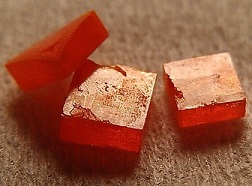
Layered inorganic semiconductors is a large class of materials composed of layers of covalently or ionically bonded atoms, with a week van der Waals bonding between the layers. This specific structure allows individual layers of these materials to be peeled off, exposing clean, dangling-bond-free surfaces. These materials include graphene (single and multi-layered), graphite (HOPG), transition metal dichalcogenides (MoS2, MoSe2, WS2, WSe2, etc), as well as phosphorene and others.
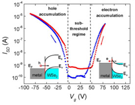
The 1-st paper reporting field-effect transistors based on this class of materials was published by us in 2004 after a lengthy delay partially caused by the Rutgers-Lucent lawyers patenting this discovery (V. Podzorov et al., "High mobility ambipolar field-effect transistors based on transition metal dichalcogenides", Appl. Phys. Lett. 84, 3301 (2004)). At the end, the patent has been awarded to Rutgers-Lucent, our paper got published and appeared before the first paper on graphene. Our patent covers transition metal dichalcogenides, as well as graphene. The irony is that only a handful of people are actually aware of this fact. Our original work, although largely unnoticed by the community, had been apparently revolutionary at that time.
The remarkable fact is that novel high-mobility inorganic FETs like these could be produced by such simple fabrication techniques as pealing/exfoliation and parylene deposition to form a high-quality semiconductor-dielectric interface (that is, not in clean room environment and w/o using expensive facilities typically used in Si technology). In addition, these devices exhibit a great performance: electron and hole mobilities in the range 100-500 cm2V-1s-1 and in many cases ambipolarity. These characteristics are easily comparable to or even better than those of commercial single-crystal Si MOSFETs that took decades to develop. The FETs based on layered materials perform so well due to their specific chemical structure: a strong in-plain bonding ensures a good delocalization of charge carriers and a high in-plain carrier mobility, while week van der Waals out-of-plane bonding ensures saturated surfaces free from dangling bonds, that would otherwise result in overwhelming deep-trap densities and dysfunctional devices.