


Latest News
1. Writing metallic nanostructures with ion beams
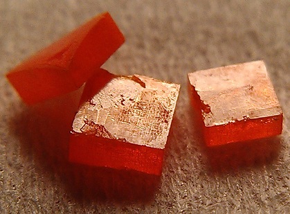
we demonstrate a simple but versatile use of a Helium Ion Microscope's (HIM) focused ion beam to fabricate conducting metallic nano- and micro-structures on arbitrary substrates of varied types and shapes. Direct patterning of pre-deposited initially discontinuous and highly insulating (> 10 TΩ/sq.) ultrathin gold or silver films with the HIM's ion beam leads to conducting continuous metallic lines with resistivities as low as 10 kΩ/sq. This relatively straightforward, high-definition technique of direct writing with an ion beam, free from complex in vacuo catalytic or precursor chemistries, opens up new opportunities for directly fabricating elements of conformal metallic nanocircuits (interconnects, resistors, and contacts) on arbitrary organic or inorganic substrates, including those with highly curved surfaces. [link].
2. Significant Joule self-heating pervasive in TFTs
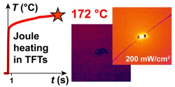
In this Perspective, recent literature on field-effect transistors based on emergent semiconducting materials, including metal-halide perovskites, conjugated polymers, and small-molecule organic semiconductors, is analyzed in terms of electric power and power density reached in transistors’ channel during their measurements. We used an in situ IR imaging to directly obtain the surface temperature distribution of biased devices under the experimental conditions commonly used in the literature. It is shown that at such conditions, the semiconducting channel would be resistively self-heated to significant temperatures, easily in excess of 150 °C. This implies a non-equilibrium device operation, possible materials’ degradation, parameter drift, and, in the best-case scenario, a non-room-temperature mobility extracted from such measurements. We show that this problem is rather common in various subfields represented in the literature, indicating that paying attention to the biasing conditions in transistor research and monitoring the local temperature of the semiconducting channel are necessary. [link].
3. Hall checklist: a practical experimental guide
Hall effect measurements are important in determining the electronic properties of emerging semiconductor materials, but care must be taken in their use and analysis. [link].
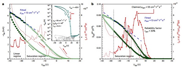
4. Safe practices of TFT mobility reporting
Accurate experimental determination of the charge carrier mobility (μ) is crucial for developing new electronic devices. Recently, a series of papers on thin-film transistors (TFTs) based on solution-coated nanocrystalline CsSnI3 and other perovskites have apparently reported erroneous TFT and Hall mobilities. Serious issues, including the nonlinear, noisy and hysteretic FET characteristics, a three-orders-of-magnitude disagreement between the Hall and FET carrier densities, and the high excitation current and Joule power densities applied in these devices, were discovered in these papers, clearly pointing to severely overestimated μ and other serious deficiencies. [link].
5. The 1st intrinsic perovskite FETs demonstrated
The intrinsic (trap-free) field-effect transistors based on epitaxial single crystalline CsPbBr3 perovskite are reported. Extensive structural, electrical, and Hall-effect characterization confirms outstanding quality of the material and a nearly ideal transistor behavior. Hole mobility of 30 cm2V-1s-1 at room temperature, monotonically increasing on cooling to 250 cm2V-1s-1 at 50 K, has been measured in these transistors. [link].
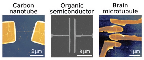
6. Water-based green lithography developed
Genuinely water-based, eco-friendly lithographic approach is demonstrated, where chitosan derivatives act as an e-beam/DUV resist. The chelation of chitosan derivatives facilitates patterning at the nanoscale without any harsh solvents or physical treatments of the surface. Both bottom-up and top-down processes are implemented directly on the surface of unconventional delicate materials, including carbon nanotubes, organic semiconductors and porcine brain microtubules. [link].
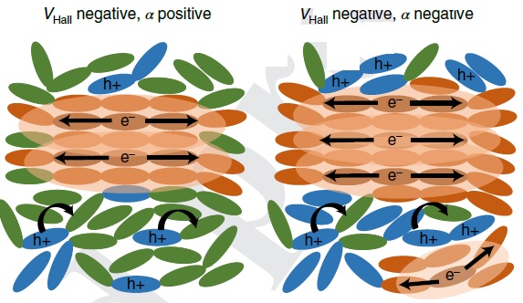
7. Carrier sign switch in polymers
Here, we show through Seebeck coefficient and Hall effect measurements, that doping π-conjugated polymers with strong electron acceptors can lead to the emergence of mobile electrons dominating the electric transport and thermo-electric properties of various polymers. Even though, as expected, holes are dominating at low doping concentrations, mobile electrons appear at heavy doping levels. Specifically, the Seebeck coefficient of several p-doped polymers changes sign from positive to negative as the concentration of the oxidizing agents FeCl3 or NOBF4 increase, and Hall effect measurements for the same p-doped polymers reveal that electrons become the dominant delocalized charge carriers. We reveal that the mechanism of this effect is based on the elimination of the transport gap at high doping concentrations. This approach of heavy p-type doping is demonstrated to provide a promising route to high-performance n-type organic thermoelectric materials. [link].
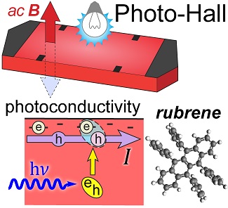
8. Photo-Hall effect in org. semicond.
The photo-Hall effect is measured for the 1st time in organic semiconductors using single crystalline rubrene as an experimental platform. These measurements allowed us to directly access the mobility and density of photocarriers generated at the surface and in the bulk of these organic crystals under a cw photoexcitation. Our data show that only mobile holes are generated in a wide range of incident light intensities. This behavior suggests that the mechanism of photoconductivity in these organic crystals is based on an interaction of long-lived, mobile triplet excitons with surface electron traps, leading to a release of mobile holes. [link].
9. Hall effect and Raman vs. strain in OFETs
The intrinsic mobility–strain relationship in single crystalline organic semiconductor rubrene has been finally revealed. It has been evaluated via the Hall effect and Raman spectra measured as a function of uniaxial mechanical strain applied to ultra-thin, bendable rubrene transistors. The study reveals a very strong, anisotropic and reversible modulation of the intrinsic (trap‐free) charge carrier mobility of single‐crystal rubrene transistors with strain, showing that the effective mobility of organic circuits can be enhanced by up to 100% with only 1% of compressive strain. Consistently, Raman spectroscopy reveals a systematic shift of the low‐frequency Raman modes of rubrene to higher (lower) frequencies with compressive (tensile) strain, which is indicative of a reduction (enhancement) of thermal molecular disorder in the crystal with strain. This study represents the first measurements of Hall effect and Raman spectra in an organic semiconductor as a function of strain. It thus lays the foundation of the strain engineering in organic electronics and advances the knowledge of the relationship between the carrier mobility, low‐frequency vibrational modes, strain, and molecular disorder in organic semiconductors. [link].
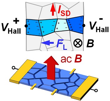
10. Hall effect in polycrystalline OFETs
The effect of grain boundaries on the Hall effect in polycrystalline organic transistors is elucidated in two exemplary systems: solution-coated C8-BTBT and thermally evaporated highly crystalline rubrene. It is shown that even when OFET mobility is as high as ~ 5 cm2V-1s-1, capacitively charged grain boundaries may lead to an underestimated Hall mobility and an overestimated Hall carrier density. [link].
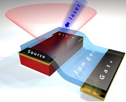
11. PL gating effect in perovskite EDLTs
We demonstrate a reversible control of photoluminescence (PL) emission from lead-halide perovskites achieved in perovskite electric-double-layer transistors (EDLTs). PL in several prototypical lead-halide perovskite compounds is shown to be reversibly tuned by a small gate voltage in the range ± 1.2 V applied to the ionic-liquid gel on the perovskite surface, with the intensity modulation that can reach one-to-two orders of magnitude. This effect may be mediated by a reversible migration of oxygen ions affecting the crystal region near the interface with the ion gel. The resulting passivation (or activation) of non-radiative recombination centers (traps) by oxygen ions would then modulate the population of mobile photogenerated electrons and holes that give rise to PL, which is thus tuned with an electric “knob” (the gate) in these devices. [link].
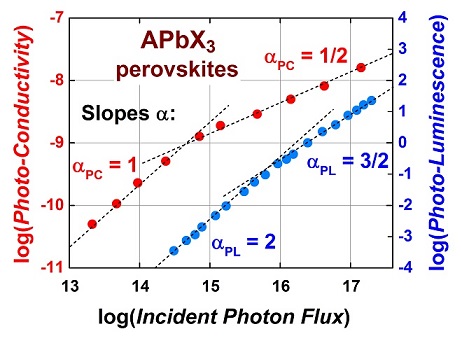
12. Correlated flux scaling in PC and PL in perovskites
Despite the rapid progress in lead-halide perovskite solar cells, understanding of the basic optoelectronic properties of these materials is lacking. Here we show a clear and universal correlation between the photoexcitation flux dependences of the photoconductivity and photoluminescence of lead-halide perovskites that contributes to phenomenological understanding of the unique photophysics of these materials. While the photoconductivity exhibits a crossover in the power-law dependence between the exponents 1 and ½, the photoluminescence exhibits a crossover between the power exponents 2 and 3/2. We discuss phenomenological scenarios leading to this unusual combination of power exponents. Specifically, an analytical model of carrier diffusion with competing bimolecular bulk recombination and surface recombination is proposed. [link].
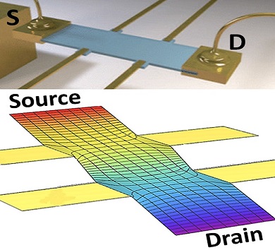
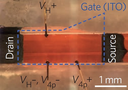
13. Artifact-free extraction of μ in 4-probe FETs
It is shown that four-probe contact geometry, frequently used for extraction of contact-corrected charge mobility in organic or inorganic semiconductors, oxides, monolayers and other emergent electronic materials, can lead to a significant mobility over-estimation due to longitudinal channel shunting by wide voltage probes. A numerical correction factor that can be used for obtaining much more accurate experimental mobilities is introduced. [link].
14. Critical assessement of mobility extraction in FETs
Mobility is an important charge-transport parameter in organic, inorganic and hybrid semiconductors. We outline some of the common pitfalls of mobility extraction from field-effect transistor (FET) measurements and propose practical recommendations to avoid reporting erroneous mobilities in publications [link].
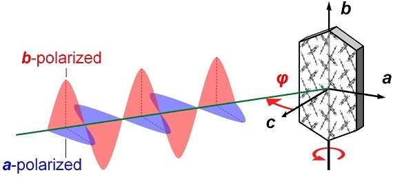
15. Polarization-dep. photo bias-stress in OFETs
Photoinduced charge transfer between semiconductors and gate dielectrics can occur in OFETs operating under illumination, leading to a pronounced bias-stress effect in devices that are normally stable while operating in the dark. Here we report an observation of a polarization dependent photoinduced bias-stress effect in two prototypical single-crystal OFETs, based on rubrene and TPBIQ. We find that the decay rate of the source-drain current in these OFETs under illumination is a periodic function of polarization angle of incident photoexcitation with respect to the crystal axes, with a periodicity of π. The angular positions of maxima and minima of the bias-stress rate match those of the optical absorption coefficient of the corresponding crystals. The analysis of the effect shows that it stems from a charge transfer of “hot” holes, photogenerated in the crystal within a very short thermalization length (<< μm) from the semiconductor-dielectric interface. The observed phenomenon is a type of intrinsic structure-property relationship, revealing how molecular packing affects parameter drift in organic transistors under illumination. We also demonstrate that a photoinduced charge transfer in OFETs can be used for recording rewritable accumulation channels of an optically defined geometry and resolution, which can be used in a number of potential applications. [link].
16. Photocarrier recombination in hybrid perovskites
We performed 1st artifact-corrected (photo) Hall effect measurements in hybrid perovskites showing that, despite the relatively low intrinsic carrier mobilities (0.5 – 60 cm2/Vs), carrier recombination in these materials is far from a Langevin type and closer to the best direct-band inorganic semiconductors, with typical electron-hole recombination coefficients in the range 10-11 – 10-10 cm3/s, but with a very long carrier diffusion (of up to 650 μm) and lifetime (of up to 2.7 ms). This can be explained by a dipolar polaronic nature of charge carriers and local defect decoration with reconfigurable dipoles [link].
17. Intrinsic carrier mobility in hybrid perovskites
Hybrid perovskites, the materials composed of an inorganic cage and organic molecular cations, have attracted widespread attention due to exceptional solar-cell efficiencies exceeding 20% recently achieved using these materials. This is a staggering performance for solution-processed semiconductors, already surpassing commercial silicon solar cells. While applied research on hybrid solar cells is fast-paced, many fundamental questions on charge carrier transport in these materials remain open. For instance, the intrinsic charge carrier mobility and the dominant transport mechanisms were not well understood. In this paper, by performing conductivity and Hall effect measurements in single crystals of hybrid perovskites, we reveal that the intrinsic charge carrier transport in these materials is limited by acoustic phonon scattering, instead of impurity scattering more common for conventional semiconductors. This observation strongly suggests that despite an apparent abundance of physical defects, the electronic defects in these solution-grown hybrid materials are effectively passivated [link].
18. "Partial" carrier coherence in org. semicon.
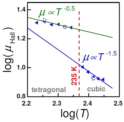
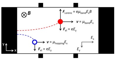
Hall effect measurements are important for elucidating the fundamental charge transport mechanisms and intrinsic mobility in organic semiconductors. However, Hall effect studies frequently reveal an unconventional behavior that cannot be readily explained with the simple band-semiconductor Hall effect model. Here, we develop an analytical model of Hall effect in organic field-effect transistors in a regime of coexisting band and hopping carriers. The model, which is supported by the experiments, is based on a partial Hall voltage compensation effect, occurring because hopping carriers respond to the transverse Hall electric field and drift in the direction opposite to the Lorentz force acting on band carriers. We show that this can lead in particular to an underdeveloped Hall effect observed in organic semiconductors with substantial off-diagonal thermal disorder. Our model explains the main features of Hall effect in a variety of organic semiconductors and provides an analytical description of Hall mobility, carrier density and carrier coherence factor [link].
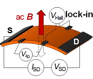
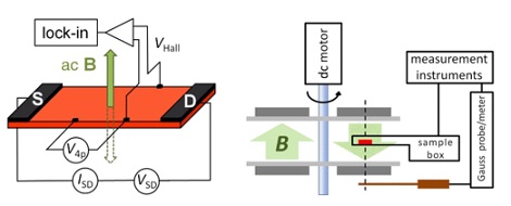
19. High-resolution ac-Hall effect methodology
A technique for high-resolution measurements of Hall effect in organic transistors utilizing a small (0.23 T) ac magnetic field is developed. These measurements allow to extend studies of the intrinsic charge carrier transport and Hall effect into systems with very low carrier mobilities of less than 1 cm2/Vs. [link].
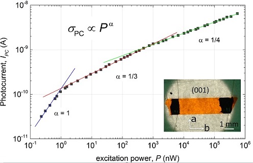
20. Non-linear photoconductivity in rubrene
Photoconductivity of an exemplary organic semiconductor rubrene is found to exhibit several distinct regimes, in which photocurrent as a function of cw (continuous wave) excitation intensity is described by a power law with exponents sequentially taking values 1, 1/3 and ¼. We show that in pristine rubrene crystals this photocurrent is generated at the very surface of the crystals, while the bulk photocurrent is drastically smaller and follows a different sequence of exponents, 1 and ½. We describe a simple experimental procedure, based on an application of the "gauge effect" in high vacuum, that allows to disentangle the surface and bulk contributions to photoconductivity. A model based on singlet exciton fission, triplet fusion and triplet-charge quenching that can describe these non-trivial effects in photoconductivity of highly ordered organic materials is proposed [link].
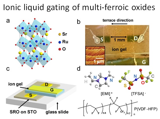
21. Ionic-liquid gating of SrRuO3
Reversible control of charge transport and magnetic properties without degradation is a key for device applications of transition metal oxides. Chemical doping during the growth of transition metal oxides can result in large changes in physical properties, but in most of the cases irreversibility is an inevitable constraint. Here we report a reversible control of charge transport, metal-insulator crossover and magnetism in field-effect devices based on ionically gated archetypal oxide system - SrRuO3 [link]. In these thin-film devices, the metal-insulator crossover temperature and the onset of magnetoresistance can be continuously and reversibly tuned in the range 90 - 250 K and 70 - 100 K, respectively, by application of a small gate voltage. We infer that a reversible diffusion of oxygen ions in the oxide lattice dominates the response of these materials to the gate electric field. These findings provide critical insights into both the understanding of ionically gated oxides and the development of novel applications.
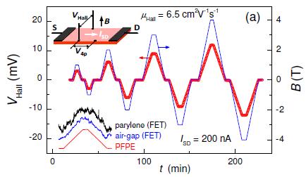
22. Trap-healing and ultra low-noise Hall effect
Fundamental studies of intrinsic charge transport properties of organic semiconductors are often hindered by charge traps associated with static disorder present even in optimized single-crystal devices. Here, we report a novel method of surface functionalization using an inert non-conjugated polymer, perfluoropolyether (PFPE, or Fomblin oil), deposited at the surface of organic molecular crystals, that results in accumulation of mobile holes and "trap healing" effect at the crystal/PFPE interface [link]. As a consequence, a remarkable ultra low-noise, trap-free conduction regime characterized by intrinsic mobility and transport anisotropy emerges in organic single crystals, and Hall effect measurements with unprecedented signal-to-noise ratio are demonstrated. This general method to convert trap-dominated organic semiconductors to intrinsic systems may enable the determination of intrinsic transport parameters with high accuracy and make Hall effect measurements in molecular crystals ubiquitous.
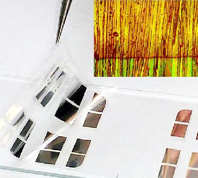
23. Extremely flexible solution-processed OFETs
Organic semiconductors are promising novel materials for applications in flexible electronics, such as bendable displays, wearable electronic fabrics and large-area printed electronics. However, in order for these materials to live up to such expectations, an outstanding resilience to mechanical strains and stresses must be demonstrated. In this article [link], we suggest a novel architecture for fabrication of ultra-thin, self-supported OFETs by crystallizing organic semiconductors (TIPS-pentacene and TES-ADT) from solutions onto extremely thin polymer membranes with pre-deposited source, drain and gate electrodes. We have performed rigorous tests of electro-mechanical stability of these devices in various experimental configurations and demonstrated that they withstand multiple bending to the radius as small as 200 μm without degradation. This is the first demonstration of high-performance, flexible organic transistors based on solution-processed small molecules, which justifies the usage of solution-processed organic semiconductors in research on flexible electronics.
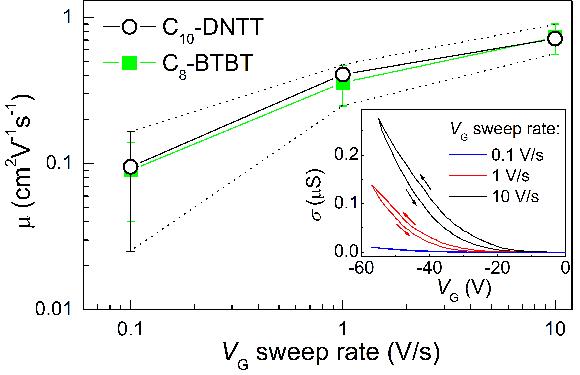
24. Dependence of μ on VG sweep rate in OFETs
In this article [link], we discuss the dynamic instability of charge carrier transport in a range of popular organic semiconductors. We observe that in many cases field-effect mobility strongly depends on the rate of the gate voltage sweep during the measurement. Some molecular systems are so dynamic that their nominal mobility can vary by more than one order of magnitude, depending on how fast the measurements are performed, making an assignment of a single mobility value to devices meaningless. It appears that dispersive transport in OFETs based on disordered semiconductors, those with a high density of localized trap states distributed over a wide energy range, is responsible for the gate voltage sweep rate dependence of nominal mobility. The paramount significance given to a single mobility value in the organic electronics community and the practical importance of OFETs for applications thus suggest that such an issue, previously either overlooked or ignored, is in fact a very important point to consider when engaging in fundamental studies of charge carrier mobility in organic semiconductors or designing applied circuits with organic semiconductors.
25. Bias stress effect in "air-gap" OFETs
Bias stress effect is currently one of the most pressing and important problems in OFET research. The intrinsic mechanisms of the effect (that is, those related only to the semiconductor properties, such as density and distribution of trap states) and non-intrinsic mechanisms (related to the dynamic processes in the dielectric layer, environmental factors or device issues) can frequently co-exist in the same device, thus making data interpretation and modeling difficult. Such entanglement between intrinsic and non-intrinsic factors results in the controversy that exists in the OFET field on this subject. In this paper [link], we have investigated bias stress effect in “air-gap” (or “vacuum-gap”) single-crystal OFETs, in which no material gate dielectric is present, and thus all the processes related to the dynamics in the dielectric layer are avoided. In addition, we could modify the density of traps in the single crystals by photo-oxidation and characterize the bias stress effect before and after this intentional modification, which thus allowed us to unambiguously relate the bias stress rate to the trap density and the effective linear field-effect mobility of the semiconductor. On the other hand, by filling the “air gap” with different types of gases, one can also investigate the intrinsic environmental effects due to the interaction of gases with the accumulation channel only. The major conclusion of this study is that in the absence of a material gate dielectric (the semiconductor-vacuum interface) the bias stress effect is caused by a relaxation of the gate-induced charge carriers in localized band tail states that are always present even in highly ordered organic crystals, and the rate of the effect strongly correlates with the density and distribution of such trap states. Polar gases (such as water or acetone vapor) introduced into the “air-gap” can also contribute to the bias stress effect through the mechanism of carrier localization by formation of charge-dipole bound states at the surface of the crystal. Given the universal existence of localized trap states in organic semiconductors, the intrinsic mechanism identified and analytically formulated here, namely the relaxation of charge carriers in the localized band tails, represents the main (possibly dominant) source of bias stress effect in the majority of OFETs, especially in disordered polycrystalline and amorphous devices.
26. Vacuum lamination approach to OFETs
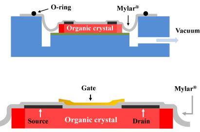
A novel vacuum lamination approach to fabrication of high-performance single-crystal organic field-effect transistors has been developed [link]. The non-destructive nature of this method allows a direct comparison of field-effect mobilities achieved with various gate dielectrics using the same single-crystal sample. The method also allows gating delicate systems, such as n-type crystals and SAM-coated surfaces, without perturbation.
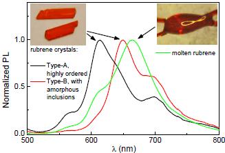
27. The origin of 650 nm PL in rubrene
Commonly observed variations in photoluminescence spectra of crystalline organic semiconductors, including appearance or enhancement of certain PL bands, are shown to originate from a small amount of structural disorder (e.g., amorphous inclusions embedded in a crystal), rather than be necessarily related to chemical impurities or material oxidation [link]. For instance, in rubrene, a minute amount of such disorder can lead to appearance of a dominant PL band at 650 nm due to triplet excitons captured and fused at these sites, with a subsequent emission from the amorphous phase. . ...
28. Photo-triggered diffusion of molecular oxygen
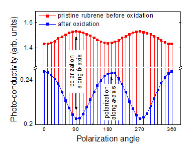
An amazing effect of diffusion of molecular oxygen in a crystalline organic semiconductor triggered by illumination is reported [link]. The study reveals that the surface of as-grown rubrene single crystals remains unoxidized, even if the crystals are stored in pure oxygen for a long period of time (in the dark). In high-quality rubrene crystals, such unperturbed state persists even if the samples are illuminated with a relatively low-intensity room light in air for many hours. However, illumination of rubrene crystals in an oxygen atmosphere with more intense white light (2-3 hours at an integrated power density 85 mW/cm2 – similar to the solar radiation) triggers a long-term oxygen diffusion that continues in the dark for hours or days, resulting in a formation of oxygen-related traps in the crystal. The depth scale of the trap distribution is ~ α-1, where α is the light absorption coefficient. Our study shows that oxygen incorporation always reduces both the dark and the photo-conductivity of rubrene, and it leads to qualitative changes in the photocurrent excitation spectra, σ(λ,θ) (see Fig. below). This method, called polarization and wavelength resolved photocurrent excitation spectroscopy (or, simply, PCE), can be used as a highly sensitive trap characterization technique for organic semiconductors.
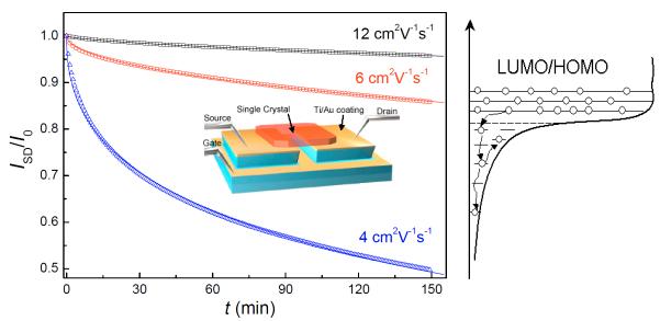
29. Bias-stress instability in OFETs
We have recently determined the origin of the bias-stress instability in single-crystal OFETs by performing a combination of transport measurements and ultraviolet photoemission spectroscopy (UPS) [link]. Bias stress instability is a monotonic decrease of the channel current under a fixed applied gate voltage. Although the microscopic origin of the effect has been intensely discussed in the community, no intrinsic (independent of device flaws or handling conditions) mechanisms have been convincingly identified. In this work, we provide experimental evidence that (in the absence of simple extrinsic factors, such as, e.g., humidity), the bias stress instability might still occur because of a ground-state charge transfer at the semiconductor/insulator interface in OFETs. As schematically depicted in the Fig. below, the rate of the effect is governed by the energetic overlap between the holes accumulated in HOMO of the semiconductor and the exponential tail of localized states in the dielectric. Our model leads to a generalized analytical description of this phenomenon in OFETs and explains all the main experimental trends of the effect, including the Vg2 dependence of the bias stress rate. This new understanding suggests that in order to improve operational stability of OFETs, the overlap between the HOMO band of a semiconductor and localized band tail of an insulator must be minimized.
30. Very large exciton diffusion length
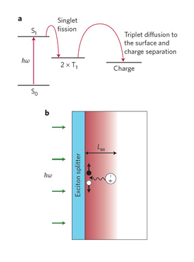
We have recently demonstrated a very large exciton diffusion length (LEX ~ 3-8 μm) in highly ordered organic crystal rubrene, implying that energy can be transported over vast distances from the bulk to the surface of the crystal, most likely by triplet excitons produced by fission of singlets [link]. This result is important because it opens a window into the fundamental understanding of the intrinsic optical properties of highly ordered organic semiconductors in hetero-structure devices. By performing polarization and wavelength resolved spectroscopy of photocurrent generated at the surface of highly pure rubrene crystals upon photoexcitation, we conclude that triplet excitons are generated with high efficiency, and suggest singlet fission as a plausible mechanism for triplet generation (see Fig. below adopted from the News & Views article by C. Silva "A little energy goes a long way", Nature Mater. 9, 884-885 (2010)). In this process, a single high-energy singlet state undergoes fission into a pair of triplets. Triplet excitons would then diffuse over distances of the order of 5 µm, as long as the material is highly ordered, which means that excitons have a high probability of reaching the surface of the crystal and dissociate.
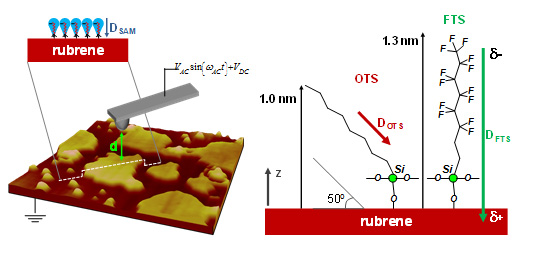
31. SAMs on organic semiconductors
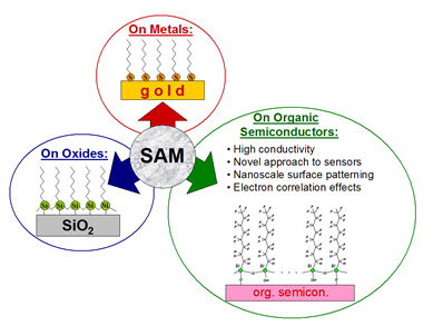
The three classes of molecular self-assembly: thiolates on metals, silanes on inorganic oxides, and silanes on organic semiconductors (see Fig. below). The 3rd class, discovered at Rutgers in 2007-2008, represents an interesting approach to surface doping, patterning and functionalization of organic semiconductors [link]. We have observed a growth of organosilane SAMs directly at the surface of organic molecular crystals. Remarkably, integrating the SAM with an organic surface results in a large increase in the surface conductivity of the semiconductor, which can be very large for SAMs with strong electron-withdrawing functional groups. For example, the 2D sheet conductivity induced by a complete monolayer of fluoroalkyl trichlorosilane (FTS, pictured in the Fig.) in rubrene crystals approaches 10-5 S per square, which is one to two orders of magnitude greater than the maximum conductivity attainable in conventional OFETs.
32. Kelvin Probe applied to SAM-rubrene system
D. J. Ellison from the group of Prof. D. C. Frisbie (University of Minnesota) successfully applied a Kelvin Probe Microscopy (KPM) to our SAM-rubrene system [link]. KPM is an AFM-based technique that can be used to map the nanoscale distribution of the surface potential in a sample. Kelvin probe microscopy of rubrene single crystals partially coated with FTS SAM revealed that the SAM coated areas are strongly negatively charged relatively to the bare rubrene surface, resulting in a very large potential difference of 0.54 V between the FTS coated and uncoated rubrene areas (see Fig. below). This provides the first microscopic confirmation of the charge-transfer mechanism of the large surface doping effect produced by the SAM at the surface of organic semiconductors.
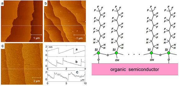
33. Microscopic mechanism of SAM nucleation
We have recently understood the microscopic mechanism of SAM nucleation and growth on organic surfaces by utilizing an AFM, a conducting-tip AFM and transport measurements. It has been observed that the SAM initially nucleates at molecular steps and other surface defects [link], when the crystal is exposed to the vapor of trichlorosilanes (see Fig. below). This is likely to occur because rubrene molecules at these defect sites are oxidized (steps may contain rubrene epoxy, hydroxyl or carboxyl groups), while the molecules on pristine flat surface of crystal terraces are not. After the nucleation, the SAM grows by the mechanism known as in-plain polymerization of silanes, which takes place along the surface via formation of Si-O-Si bridges between the adjacent SAM molecules (see our model below). Interestingly, the observed effect of molecular step "decoration" is accompanied by a strong local doping effect resulting in macroscopically long conducting paths of nanoscale width (a single crystalline analogue of organic nanowires) that can span distances of up to ~ 1 cm at the surface of the sample between electrical contacts. The observed decoration of molecular steps opens intriguing possibilities for visualization, passivation, and selective doping of surface and interfacial defects in organic electronic devices and provides a novel system for the studies of nanoscale charge transport in organic conductors.
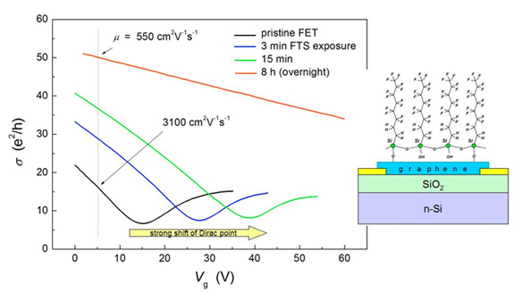
34. FTS SAM on single-layer graphene FETs
We have realized a high-density hole-doped regime by growing FTS SAM on top of the single-layer graphene FETs (n-Si gate underneath) (see Fig. below) [link]. It was observed that a stable and complete self-assembled monolayer of alkyl-silane can be grown at the surface of graphite and graphene. Detailed characterization of the system using scanning probe microscopy, X-ray photoelectron spectroscopy, and transport measurements revealed the monolayer structure and its effect on the electronic properties of graphene. The monolayer induces a strong surface doping with a high density of mobile holes (> 1013 cm-2). The ability to tune electronic properties of graphene via stable molecular self-assembly, including selective doping of steps, edges, and other defects, may have important implications in future graphene electronics. This system represents an example of integration of organic and inorganic electronic materials resulting in novel functionalities.