|

DEPARTMENT OF PHYSICS AND
ASTRONOMY
LINKS
|
Basics: Direct and Inverse Photoemission
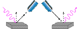 Photoemission
and inverse photoemission are two highly complementary techniques
that provide a detailed understanding of the electronic structure
above and below the Fermi level. Photoemission is based on the
familiar photoelectric effect. In simplest terms, one measures the
energy and angular distributions of electrons emitted from a sample
that is excited by monochromatic light. Operationally, inverse
photoemission is the time reversed process of photoemission, where
monoenergetic electrons impinge on a sample and the emitted photons
are detected. Experimental implementation is illustrated
schematically in the figure above. Photoemission
and inverse photoemission are two highly complementary techniques
that provide a detailed understanding of the electronic structure
above and below the Fermi level. Photoemission is based on the
familiar photoelectric effect. In simplest terms, one measures the
energy and angular distributions of electrons emitted from a sample
that is excited by monochromatic light. Operationally, inverse
photoemission is the time reversed process of photoemission, where
monoenergetic electrons impinge on a sample and the emitted photons
are detected. Experimental implementation is illustrated
schematically in the figure above. |
Sample Results: Direct and Inverse Photoemission
Metallic quantum well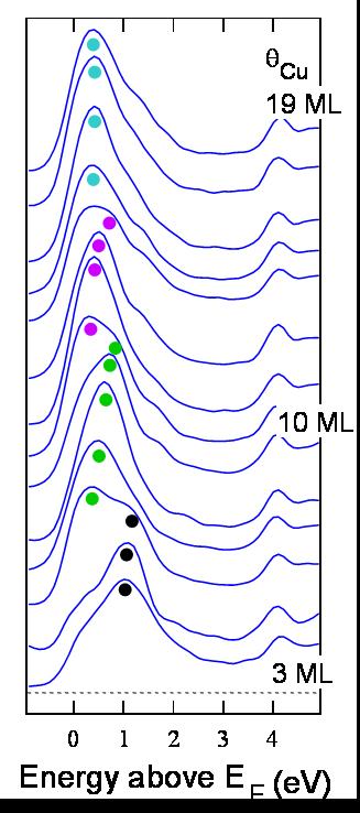 states in the Cu/fccFe/Cu(100) system:
The figure on the left is a
series of normal emission photoemission spectra obtained from a Cu
wedge grown on a 5 ML fccFe/Cu(100) structure. Spectra from
different positions on the wedge (which correspond to different
thicknesses of the Cu overlayer) are displayed as an intensity plot.
Dark colors indicate low
states in the Cu/fccFe/Cu(100) system:
The figure on the left is a
series of normal emission photoemission spectra obtained from a Cu
wedge grown on a 5 ML fccFe/Cu(100) structure. Spectra from
different positions on the wedge (which correspond to different
thicknesses of the Cu overlayer) are displayed as an intensity plot.
Dark colors indicate low
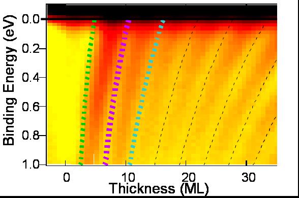 intensity,
bright yellow indicates high intensity. The bright bands moving
towards the Fermi level with increasing Cu thickness are the
metallic quantum well (MQW) states in the Cu overlayer.
The figure at the
As suggested by the discussion above, as the thickness of a metallic
quantum well changes, MQW state energies change. The figure above on
the left shows a series of inverse photoemission spectra obtained
from the Cu/fccFe/Cu(100) system as a function of increasing film
thickness. The tick marks show that MQW states move upward with
increasing thickness. The figure at the right shows normal incidence
IPS spectra from planar Cu/fccFe/Cu(100) structures with increasing
Cu thickness. The occupied MQW states highlighted by each
color in the photoemission data is seen above the Fermi level in the
IPS data. intensity,
bright yellow indicates high intensity. The bright bands moving
towards the Fermi level with increasing Cu thickness are the
metallic quantum well (MQW) states in the Cu overlayer.
The figure at the
As suggested by the discussion above, as the thickness of a metallic
quantum well changes, MQW state energies change. The figure above on
the left shows a series of inverse photoemission spectra obtained
from the Cu/fccFe/Cu(100) system as a function of increasing film
thickness. The tick marks show that MQW states move upward with
increasing thickness. The figure at the right shows normal incidence
IPS spectra from planar Cu/fccFe/Cu(100) structures with increasing
Cu thickness. The occupied MQW states highlighted by each
color in the photoemission data is seen above the Fermi level in the
IPS data.
HOMO and LUMO level
alignment
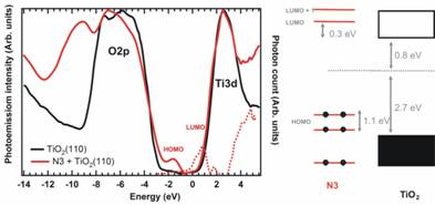 for
the N3 dye molecule on the TiO2(110) surface:
The most efficient dye sensitized solar
cells
(DSSCs) to date are fabricated with anatase titania nano-particles
sensitized with N3 dye.
The alignment of the N3 HOMO and LUMO levels with the conduction
band minimum (CBM) and valence band maximum (VBM) of the underlying
titania semiconductor is
critical for solar cell performance. Using our unique
apparatus that houses both photoemission in the same experimental
chamber, we can study the level alignment from the model
N3/rutile-TiO2(110) system. for
the N3 dye molecule on the TiO2(110) surface:
The most efficient dye sensitized solar
cells
(DSSCs) to date are fabricated with anatase titania nano-particles
sensitized with N3 dye.
The alignment of the N3 HOMO and LUMO levels with the conduction
band minimum (CBM) and valence band maximum (VBM) of the underlying
titania semiconductor is
critical for solar cell performance. Using our unique
apparatus that houses both photoemission in the same experimental
chamber, we can study the level alignment from the model
N3/rutile-TiO2(110) system.
Band alignment in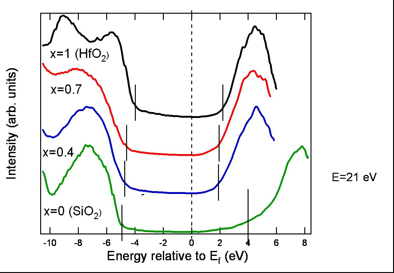 high-K dielectric/semiconductor systems:
As scaling in the semiconductor industry moves towards critical
dimensions of ~ 45 nm, the effective oxide thickness needed for
metal semiconductor oxide (MOS) devices approaches 1 nm. At
these thicknesses, the leakage current through an SiO2 oxide is
unacceptably large, and high-K dielectrics such as HfO2
are now being employed. Band alignment between the oxide and
the semiconductor, as well as between a candidate metal gate and the
oxide, can be measured. The figure at the left shows combined
photoemission and inverse photoemission spectra that give the band
gap for HfO2, HfSiOx, and SiO2.
high-K dielectric/semiconductor systems:
As scaling in the semiconductor industry moves towards critical
dimensions of ~ 45 nm, the effective oxide thickness needed for
metal semiconductor oxide (MOS) devices approaches 1 nm. At
these thicknesses, the leakage current through an SiO2 oxide is
unacceptably large, and high-K dielectrics such as HfO2
are now being employed. Band alignment between the oxide and
the semiconductor, as well as between a candidate metal gate and the
oxide, can be measured. The figure at the left shows combined
photoemission and inverse photoemission spectra that give the band
gap for HfO2, HfSiOx, and SiO2.
Read more:
Unoccupied electronic structure of Ru(0001),
W.-K. Siu and R.A. Bartynski, Phys.
Rev. B, 75, 235427 (2007)
|
Recent Publications
(back to top)
-
Unoccupied electronic structure of Ru(0001)
K. Siu, and R. A. Bartynski, Phys. Rev. B 75, 235427 (2007)
-
Room temperature ferromagnetism in Mn ion
implanted epitaxial ZnO films
D.H.Hill, D.A. Arena,
R.A. Bartynski, P. Wu, G. Saraf, Y. Lu, Wielunski, R. Gateau, J.
Dvorak, A. Moodenbaugh, and Y.K. Yeo, Physica Status Solidi A,
203, 3836 (2006)
-
Ferromagnetism in Fe-implanted a-plane ZnO
Films
D.P. Wu, G. Saraf, Y. Lu, D.H. Hill, D.A. Arena, R.A. Bartynski, L.
Wielunski, R. Gateau, J. Dvorak, A. Moodenbaugh, T. Siegrist, J.
A. Raley, and Yung Kee Yeo, Appl. Phys. Lett.89, 12508
(2006)
-
The relation between crystalline phase,
electronic structure, and dielectric properties in high-k gate
stacks
S.
Sayan, M. Croft, N.C. Nguyen, T. Emge, J. Ehrstein, I. Levin, J.
Suehle, R.A. Bartynski, and E. Garfunkel, AIP Conf. Proc. 788,
92 (2005)
-
Dichroic effects in Auger-photoelectron
coincidence spectroscopy of solids
R.
Gotter, F. Da Pieve. A. Ruocco, F. Offi, G. Stefani, R.A.
Bartynski, Phys. Rev. B. 72, 235409 (2005)
-
Inverse Photoemission Spectroscopy from
Al(100)
J. F. Veyan, W. Ibanez, R.A.
Bartynski, P Vargas, and P. Haberle, Phys. Rev. B. 71,
155416 (2005)
|
|