|

DEPARTMENT OF PHYSICS AND
ASTRONOMY
LINKS
|
Basics: High-K dielectrics for nanoelectronics applications
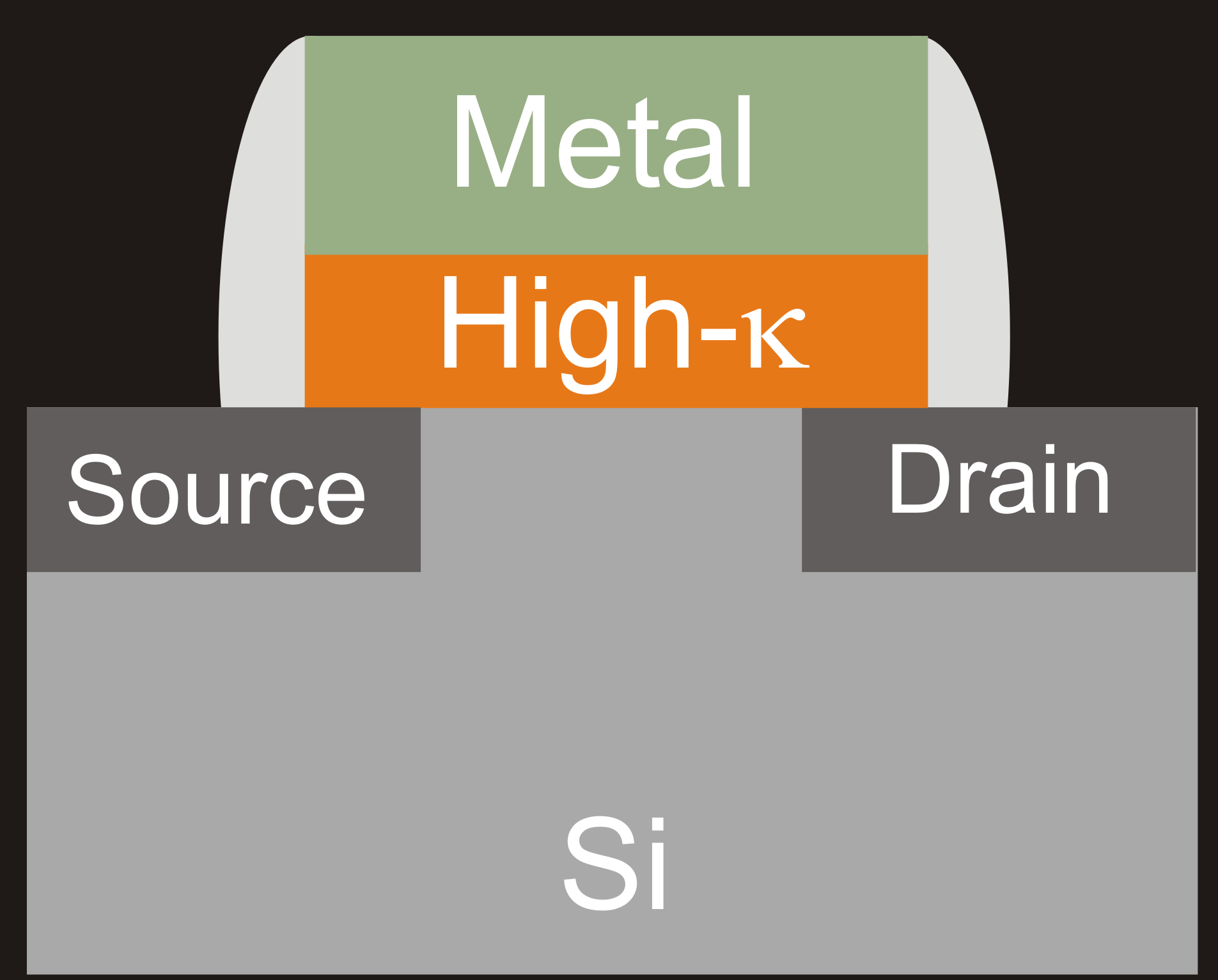 The
replacement of SiO2 gate dielectrics and poly-Si gate electrodes
with high-K gate dielectrics and metal gate electrodes are two of
the most pressing upgrades that the MOSFET must undergo in order for
scaling to continue at its current pace. The band offsets of the
metal gate/high-K dielectric stacks are critical to the success of
these devices, as they are the barrier heights which resist the
transfer of electrons and holes across the gate dielectric, i.e.
gate leakage current. We use a combination of UV photoemission and
inverse photoemission spectroscopies (UPS, IPS) in the same vacuum
chamber to measure the occupied and unoccupied densities of states
of thin film oxide/semiconductor samples, from which measurements we
determine valence and conduction band offsets (VBO, CBO) between the
dielectric and the semiconductor. By sequentially depositing metal
in situ, and performing UPS and IPS between depositions, we also can
determine the VBO and CBO between the metal and dielectric layers.
In addition, we have performed similar photoemission measurements at
higher photon energies at beamline U5 of the National Synchrotron
Light Source to observe the core levels of these materials as well
as the valence bands. The
replacement of SiO2 gate dielectrics and poly-Si gate electrodes
with high-K gate dielectrics and metal gate electrodes are two of
the most pressing upgrades that the MOSFET must undergo in order for
scaling to continue at its current pace. The band offsets of the
metal gate/high-K dielectric stacks are critical to the success of
these devices, as they are the barrier heights which resist the
transfer of electrons and holes across the gate dielectric, i.e.
gate leakage current. We use a combination of UV photoemission and
inverse photoemission spectroscopies (UPS, IPS) in the same vacuum
chamber to measure the occupied and unoccupied densities of states
of thin film oxide/semiconductor samples, from which measurements we
determine valence and conduction band offsets (VBO, CBO) between the
dielectric and the semiconductor. By sequentially depositing metal
in situ, and performing UPS and IPS between depositions, we also can
determine the VBO and CBO between the metal and dielectric layers.
In addition, we have performed similar photoemission measurements at
higher photon energies at beamline U5 of the National Synchrotron
Light Source to observe the core levels of these materials as well
as the valence bands. |
Recent Highlights: High-K dielectrics
Room temperature
reduction of HfO2/Ge interfacial oxide upon deposition of
Al
With the trend towards the use of these
alternative gate dielectric materials, and the departure from
reliance on the Si/SiO2 interface, Ge has emerged as an
attractive candidate semiconductor material for next-generation MOS
devices, but material stability and band at the high-K interface are
critical issues for successful implementation of this technology. In this work, we study the stability of a HfO2/GeOx/Ge
stacks upon Al deposition at 300 K, studied using synchrotron X-ray
photoemission spectroscopy (XPS), ultra-violet photoemission
spectroscopy (UPS) and inverse photoemission spectroscopy (IPS). We
have d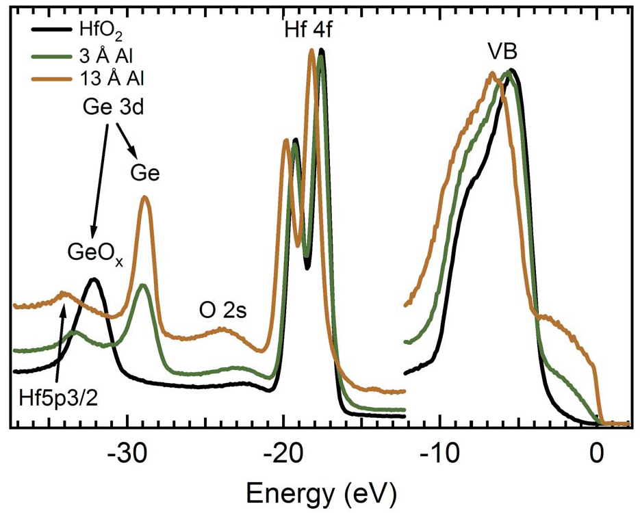 etermined that the high-K/Ge VBO = 3.0 eV, the CBO = 2.0 eV,
and the oxide bandgap is 5.7 eV in good agreement with earlier
photoemission and internal photoemission measurements. Surprisingly,
we find that the Al oxidizes immediately upon deposition, but not at
the expense of reducing the HfO2 film. Rather, the
interfacial GeOx is reduced upon metallization. This
process occurs even at room temperature. The deposition of additional
Al results in elimination of the interface oxide, metallic overlayer
growth, and establishing an electric field across the oxide, but no
apparent reduction of the HfO2 film. etermined that the high-K/Ge VBO = 3.0 eV, the CBO = 2.0 eV,
and the oxide bandgap is 5.7 eV in good agreement with earlier
photoemission and internal photoemission measurements. Surprisingly,
we find that the Al oxidizes immediately upon deposition, but not at
the expense of reducing the HfO2 film. Rather, the
interfacial GeOx is reduced upon metallization. This
process occurs even at room temperature. The deposition of additional
Al results in elimination of the interface oxide, metallic overlayer
growth, and establishing an electric field across the oxide, but no
apparent reduction of the HfO2 film.
The figure at the left shows SXPS spectra as Al is sequentially
deposited on the HfO2/GeOx/Ge sample.
With only 3Ang Al, the Ge core levels show that the interfacial GeOx
is almost completely reduced. Moreover, there is no
appreciable change in the Hf core levels indicating that HfO2
is not reduced in this process. Spectra of the Al 2p core
level (not shown) indicate only oxidized Al is present.
Upon deposition of additional Al, metallic emission is seen at the
Fermi level, the HfO2 features are all shifted by 0.7 eV
away from the Fermi level (creating a field across the oxide), and
further reduction of the HfO2/Ge interface occurs.
Read more:
GeOx interface layer reduction upon Al-gate deposition on a HfO2/GeOx/Ge(001) stack
S.Rangan, E.J. Bersch, R.A. Bartynski,
and E. Garfunkel, Applied Physics Letters Appl. Phys. Lett.92, 172906 (2008)
|
Recent Publications
(back to top)
-
Electron Spectroscopic Measurements of Band Alignment in Metal/Oxide/Semiconductor Stacks
S. Rangan, E. Bersch, R.A. Bartynski, E. Garfunkel and E. Vescovo, ECS Transactions,
33, 267 (2010)
-
Band offsets of a ruthenium gate on ultra-thin high-K oxide films on silicon
S. Rangan, E. Bersch, R.A. Bartynski, E. Garfunkel and E. Vescovo, Physical Review B,
79,075106 (2009)
-
Band offsets of ultrathin high-K oxide films with silicon
E. Bersch, S. Rangan, R.A. Bartynski, E. Garfunkel and E. Vescovo, Physical Review B,
78, 085114 (2008)
-
GeOx interface layer reduction upon Al-gate deposition on a HfO2/GeOx/Ge(001) stack
S. Rangan, E. Bersch, R.A. Bartynski, E. Garfunkel and E. Vescovo, Appl. Phys. Lett.92, 172906
(2008)
-
The relation between crystalline phase, electronic structure, and
dielectric properties in high-k gate stacks
S.
Sayan, M. Croft, N.C. Nguyen, T. Emge, J. Ehrstein, I. Levin, J.
Suehle, R.A. Bartynski, and E. Garfunkel, AIP Conf. Proc. 788,
92 (2005)
|
|