
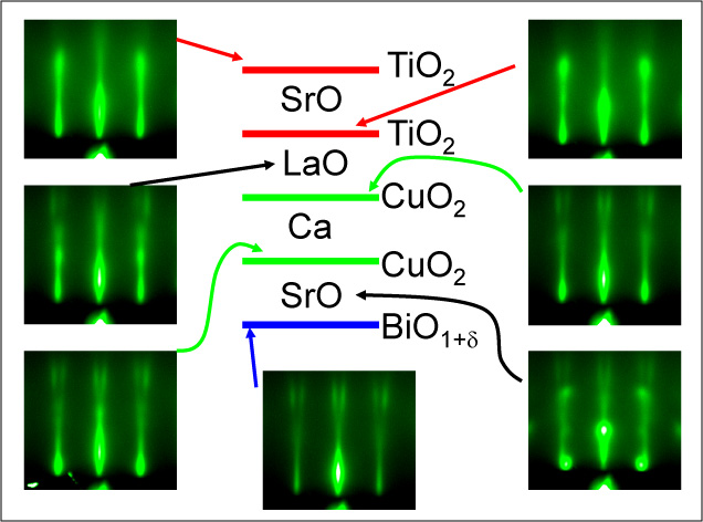
Atomically-controlled Quantm OxidesAtomic-scale or nano-scale heterostructure engineering in IV, III-V and II-VI semiconductors, and elemental metals has led to many discoveries and developments such as fractional quantum Hall effect, semiconductor lasers, giant magnetoresistance and magnetic tunnel junctions. The key player behind this success is the Molecular Beam Epitaxy (MBE) technique, with which one can grow arbitrary heterostructures of atomic-precision. One of the main efforts in our group is to extend the realm of this proven technology to a newly-emerging and less-explored material system, the complex oxides. Complex oxides exhibit much more copious electronic properties than do the conventional semiconductors and the elemental metals, such as semiconducting, high Tc superconducting, colossal magnetoresistive, (half-)metallic, (anti-)ferromagnetic, ferro(para, piezo, pyro)electric, and multiferroic behaviors. Furthermore, researchers have already demonstrated that when two complex-oxide systems are interfaced with each other, multifunctional, or sometimes completely new, properties tend to emerge. This suggests that if we apply the atomic-scale heterostructure engineering scheme to this complex oxide material system, we may discover many more novel properties and applications. However, compared with the conventional semiconductor and metal MBE's, complex-oxide MBE requires much higher level of technical sophistication. In order to tackle this problem effectively, we have built a unique oxide-MBE system , and utilizing the new oxide-MBE system and drawing on the strong theoretical and characterization support of other Rutgers groups, we will synthesize and study nanostructured oxide "metamaterials" and search for novel functionalities in these emerging territories. Figure: Reflection High Energy Electron Diffraction (RHEED) images showing atomic-layer sequence of an artificial complex-oxide interface Nano/micro Oxide Devices As complementary tools to the atomic-precision oxide-MBE technique, we make use of other thin film growth techniques such as PLD (Pulsed Laser Deposition), CVD (Chemical Vapor Deposition), Ion Beam Assisted Deposition (IBAD) and Sputtering. Each of these techniques has its own advantages for certain applications, and we utilize each technique for different applications.On many of the thin film systems created by one of these growth techniques, we routinely create nano/micro-device structures by relevant lithography techniques and investigate their electronic properties such as strongly-correlated artificial 2D electron gas, artificial high Tc superconductors, magnetism-superconductivity proximity effect, artificial ferroelectrics and multiferroics, ferroelectric/magnetic tunnel junctions, electric/spin field effect, and spin- injection Josephson effect. Materials Research for Superconducting Quantum Computers In parallel with the oxide metamaterials efforts, we also conduct materials research for superconducting quantum computers. Superconducting quantum computers based on Josephson junctions have been the recent focus of many researchers in quantum computation due to their scalable architecture.However, as Prof. Oh and his collaborators have demonstrated, amorphous materials routinely used for the tunnel barriers and the wiring dielectrics are a major source of decoherence, which seriously deteriorates the performance of superconducting quantum computers. This suggests that it is essential to develop highly coherent materials before realization of practical superconducting quantum computers. As a pioneer in this field, we are investigating the role of material disorder as a decoherence mechanism and searching for advanced materials for coherent superconducting quantum computers. This project is a joint effort with National Institute of Standards and Technology (NIST), Colorado.
|
![]()
[HOME][RESEARCH][PUBLICATIONS][PEOPLE][LINKS]
Copyright(c) 2008 Rutgers University.