| Our
shared nano-fabrication facilities include a class 100 cleanroom, an
electron-beam lithography
system
based on the thermal-field-emitter SEM Sirion (FEI Company) equipped
with an e-beam writing attachment (J C Nabity Lithography
Systems), and three thin-film deposition systems for magnetron
sputtering, thermal evaporation, and electron-gun deposition of thin
films of metals and dielectrics. Other equipment available includes a
reactive ion etcher, a scanning probe microscope, photomask aligner,
optical microscope, and other equipment required for wafer and sample
processing. |

Thermal-field
emitter SEM system
(FEI Sirion
equipped with JC Nabity
Lithography Systems)
|
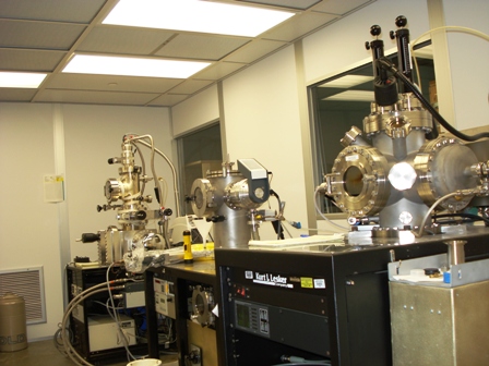
Thin-film
deposition systems (magnetron sputtering,
thermal
evaporation
and e-gun deposition)
|
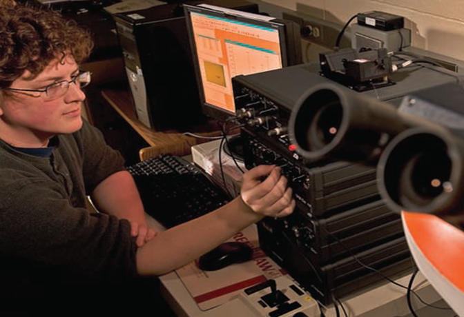
Micro-Raman, Renishaw in-via with 514 nm, 635 nm & 785 nm
lasers
|
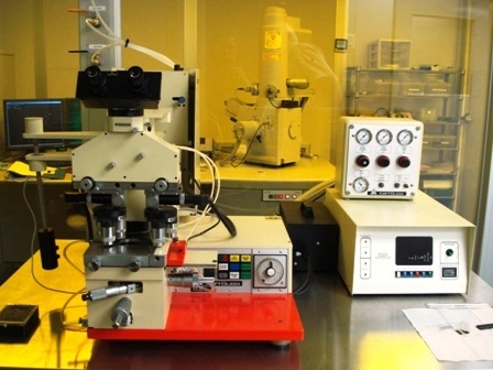
Photomask
alignment system (Karl Suss, 100DU030) |
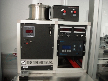
Reactive
Ion Etching system (Torr Inc., RIE300W-3MFC) |
|
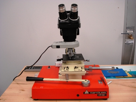
Wafer
scriber (Karl Suss,
HR-50)
|
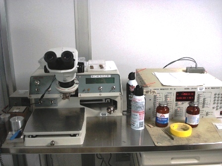
Wire
bonding machine
(West Bond,
7476D-79)
|
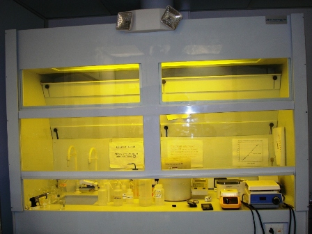
Wet
chemical bench (2M Airtechnology)
|
|
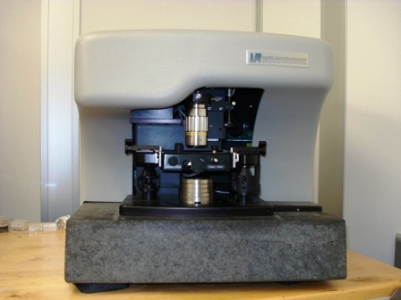
Scanning
probe microscope
(Pacific Nanotechnologies, Nano-R SPM)
|
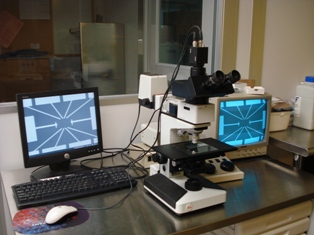
Optical
microscope
(Leitz
Wetzler, Labor Lux S)
|
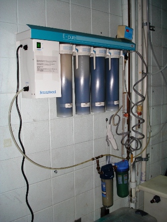
Water
purification system
(Barnstead, E-Pure)
|