Rutgers Physics Student Response System
During the polling period, when the PC has relinquished control, the state is controlled by a digital clock driven at one megahertz. This clock has an inner cycle which counts from 0 to 792. A program in Rom is addressed by these lines and controls the state of the system. Upon reaching 792 this inner cycle resets itself and steps the outer 6 bit clock, given by the D lines which control which column on the student stations is active.
The microprogram executed on each minor cycle first sets the ram to output the LED status for each substation in turn, and outputs the LED latch pulse for that substation. This turns on the appropriate LEDs. It then cycles through the 24 combinations of three substations and eight subsubstations, reading the status of the row lines through the multiplexers. At each point one substation is being polled by the lower nibble and one by the upper nibble of the byte-wide data lines. The program then enters a dormant state for the appropriate time, during which the system is doing nothing except lighting the appropriate lights. After this period, which is most of the cycle, it turns off all lights, and then terminates the minor cycle, incrementing the count on D0-D5, the major cycle.
The major cycle, indexed by the D lines, starts at 0 for the first student station and the right column. After reaching 48 it is addressing nonexistent columns and has no effect. But shortly thereafter the PC will experience the clock interrupt, and will take control, transfer the data, and reset the clocks.
More detailed information is available. The controller currently in use is a wire-wrapped board, though it is in the process of being replaced by a new design on PC boards. For the wire-wrapped version, we have the clock circuit diagram and the diagram for the rest of the controller. a complete list of chips and connections. For the new PC board version, which is on three boards, the documentation is separate for each piece. We have the circuit diagrams for part a, part b,, but not for part c (sorry). There are separate complete lists of pins and connections, part a, part b, and part c, and PC board layouts for part a, part b, and part c. Also available are the details of the microprogram in ROM and allocation of RAM addresses. [Please note: the controller was previously called Boss2 and before that just Boss. Thses old names remain on some of these references.]
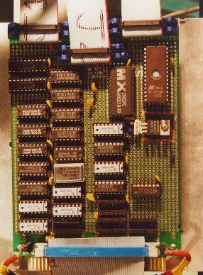
In a dramatically different spirit, we also provide a picture of the controller, wire wrapped version.