|

DEPARTMENT OF PHYSICS AND
ASTRONOMY
LINKS
|
Basics: Scanning Tunneling Microscopy
 Scanning
probe microscopy has revolutionized the study of the structure,
growth, morphology, and electronic structure of surfaces, thin films
and nanostructures. We use an Omicron VT-SPM to study the growth of
ultrathin metal overlayers on metal surface that exhibit quantum
size effects, metal overlayer morphology, and the adsorption of
organics molecules on a variety of surfaces. We also study the
spatially resolved electronic properties of these systems. The
instrument has a separate sample preparation with a loadlock for
rapid sample and tip introduction. The preparation chamber includes
metal and organic molecule deposition capabilities, as well as a
range of surface characterization techniques such as LEED, Auger
spectroscopy and XPS. Scanning
probe microscopy has revolutionized the study of the structure,
growth, morphology, and electronic structure of surfaces, thin films
and nanostructures. We use an Omicron VT-SPM to study the growth of
ultrathin metal overlayers on metal surface that exhibit quantum
size effects, metal overlayer morphology, and the adsorption of
organics molecules on a variety of surfaces. We also study the
spatially resolved electronic properties of these systems. The
instrument has a separate sample preparation with a loadlock for
rapid sample and tip introduction. The preparation chamber includes
metal and organic molecule deposition capabilities, as well as a
range of surface characterization techniques such as LEED, Auger
spectroscopy and XPS. |
Sample Results: Scanning Tunneling Microscopy
More Details: STM
(back to top)
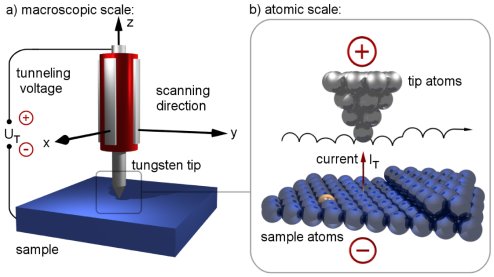 The
basic principles and implementation of STM are illustrated at the
right. A sharp tip is placed in close proximity of the sample
surface. A small bias is applied to the tip (either + or - ) and
when the tip is within a few Angstrom of the surface, a tunneling
current will flow. In contrast to the image at the right, a tip is
rarely sharpened to atomic dimensions in a controlled manner.
Typically a tip is chemically etched to a radius of several
nanometers, and it is from the small asperities that provide the
ability for atomic resolution. The tip is affixed to a piezoelectric
tube with electrodes. Applying a high voltage across opposite
electrodes cause a small distortion of the piezoelectric tube and
thus effects the in-plane motion of the tip needed for scanning
(i.e., x-y motion) and distortion along the axis of the tube (i.e.
z-motion). While the tip is scanned, the tunneling current is
monitored and fed into a feedback loop that controls the voltage
applied to the z-piezo. Images are usually obtained in either of two
modes. In the constant current mode, illustrated in the figure at
the right, a fixed voltage is applied between the tip and the sample
while the feedback loop adjusts the z-piezo so as to maintain
constant tunneling current as the tip is scanned across the surface.
As the tunneling current depends exponentially on the tip-sample
distance, the tip is maintained at a constant height above the
surf The
basic principles and implementation of STM are illustrated at the
right. A sharp tip is placed in close proximity of the sample
surface. A small bias is applied to the tip (either + or - ) and
when the tip is within a few Angstrom of the surface, a tunneling
current will flow. In contrast to the image at the right, a tip is
rarely sharpened to atomic dimensions in a controlled manner.
Typically a tip is chemically etched to a radius of several
nanometers, and it is from the small asperities that provide the
ability for atomic resolution. The tip is affixed to a piezoelectric
tube with electrodes. Applying a high voltage across opposite
electrodes cause a small distortion of the piezoelectric tube and
thus effects the in-plane motion of the tip needed for scanning
(i.e., x-y motion) and distortion along the axis of the tube (i.e.
z-motion). While the tip is scanned, the tunneling current is
monitored and fed into a feedback loop that controls the voltage
applied to the z-piezo. Images are usually obtained in either of two
modes. In the constant current mode, illustrated in the figure at
the right, a fixed voltage is applied between the tip and the sample
while the feedback loop adjusts the z-piezo so as to maintain
constant tunneling current as the tip is scanned across the surface.
As the tunneling current depends exponentially on the tip-sample
distance, the tip is maintained at a constant height above the
surf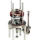 ace in this mode. Therefore, by monitoring the displacement of
the Omicron VT-STM z-piezo during scanning, a topographic image of
the surface
is produced. The other common mode is the constant-z mode. In this
mode, the z-position of the tip is fixed in space as the tip is
scanned across the sample with a constant tunneling bias. As
features of the surface are encountered, the tunneling current will
vary with the tip-sample distance and can be recorded to form an
image of the surface. This second mode emphasizes that the STM is
sensitive to the electronic structure of the surface and therefore
images do not necessarily correspond to true surface morphology.
However, this sensitivity to electronic structure can be used to
obtain real-space images of the surface charge density, as well as
to aide in the identification of different chemical species on the
surface. ace in this mode. Therefore, by monitoring the displacement of
the Omicron VT-STM z-piezo during scanning, a topographic image of
the surface
is produced. The other common mode is the constant-z mode. In this
mode, the z-position of the tip is fixed in space as the tip is
scanned across the sample with a constant tunneling bias. As
features of the surface are encountered, the tunneling current will
vary with the tip-sample distance and can be recorded to form an
image of the surface. This second mode emphasizes that the STM is
sensitive to the electronic structure of the surface and therefore
images do not necessarily correspond to true surface morphology.
However, this sensitivity to electronic structure can be used to
obtain real-space images of the surface charge density, as well as
to aide in the identification of different chemical species on the
surface.Read more:
Direct determination of HOMO and LUMO band alignment for N3 dye and isonicotinic acid on TiO2(110) and ZnO(11-20),
S. Rangan, E.J. Bersch, J.-P. Theisen, and
R.A. Bartynski, Science, (submitted)
|
Recent Publications
(back to top)
-
Room temperature ferromagnetism in Mn ion
implanted epitaxial ZnO films
D.H.Hill, D.A. Arena,
R.A. Bartynski, P. Wu, G. Saraf, Y. Lu, Wielunski, R. Gateau, J.
Dvorak, A. Moodenbaugh, and Y.K. Yeo, Physica Status Solidi A,
203, 3836 (2006)
-
Ferromagnetism in Fe-implanted a-plane ZnO
Films
D.P. Wu, G. Saraf, Y. Lu, D.H. Hill, D.A. Arena, R.A. Bartynski, L.
Wielunski, R. Gateau, J. Dvorak, A. Moodenbaugh, T. Siegrist, J.
A. Raley, and Yung Kee Yeo, Appl. Phys. Lett.89, 12508
(2006)
-
The relation between crystalline phase,
electronic structure, and dielectric properties in high-k gate
stacks
S.
Sayan, M. Croft, N.C. Nguyen, T. Emge, J. Ehrstein, I. Levin, J.
Suehle, R.A. Bartynski, and E. Garfunkel, AIP Conf. Proc. 788,
92 (2005)
-
Dichroic effects in Auger-photoelectron
coincidence spectroscopy of solids
R.
Gotter, F. Da Pieve. A. Ruocco, F. Offi, G. Stefani, R.A.
Bartynski, Phys. Rev. B. 72, 235409 (2005)
-
Inverse Photoemission Spectroscopy from
Al(100)
J. F. Veyan, W. Ibanez, R.A.
Bartynski, P Vargas, and P. Haberle, Phys. Rev. B. 71,
155416 (2005)
|
|
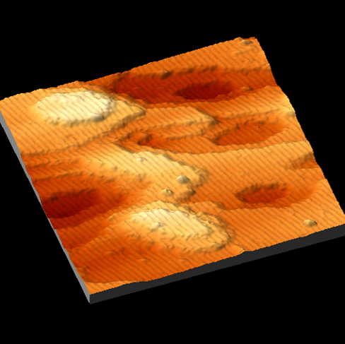
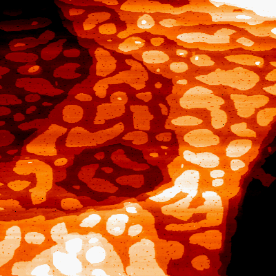
 The
stoichiometric rutile TiO2(110) surface (30nm x 30nm) and
(6nm x 6nm):
SBy an appropriate sequence of sputtering and annealing in ultrahigh
vacuum, an atomically clean and well ordered TiO2(110)
surface can be prepared and imaged in UHV. The bright rows are
assigned to the bridging oxygen ions in what is essentially a
bulk-truncated geometry. This has been our starting surface for
studies of organic dyes on oxide surfaces relevant to dye sensitized
solar cells.
The
stoichiometric rutile TiO2(110) surface (30nm x 30nm) and
(6nm x 6nm):
SBy an appropriate sequence of sputtering and annealing in ultrahigh
vacuum, an atomically clean and well ordered TiO2(110)
surface can be prepared and imaged in UHV. The bright rows are
assigned to the bridging oxygen ions in what is essentially a
bulk-truncated geometry. This has been our starting surface for
studies of organic dyes on oxide surfaces relevant to dye sensitized
solar cells.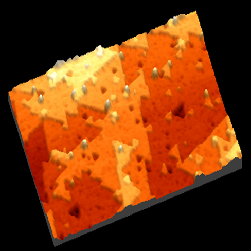 Cu
islands on the ZnO(0001) surface (100nm x 30nm):
Step edges on the Zn(001) surface form a characteristic pattern
reflecting the 3-fold symmetry of the basal plane of the wurtzite
structure. Triangular islands or vacancy pits of sequential
atomic layers are rotated by 180. Cu neither wets the surface
nor disrupts the surface morphology. Rather, 3-dimensional Cu
islands, typically 30 A in diameter and 8 A tall, form.
Cu
islands on the ZnO(0001) surface (100nm x 30nm):
Step edges on the Zn(001) surface form a characteristic pattern
reflecting the 3-fold symmetry of the basal plane of the wurtzite
structure. Triangular islands or vacancy pits of sequential
atomic layers are rotated by 180. Cu neither wets the surface
nor disrupts the surface morphology. Rather, 3-dimensional Cu
islands, typically 30 A in diameter and 8 A tall, form.