Home
About Us
We are an experimental materials physics group at Rutgers, the State University of New Jersey, Department of Physics & Astronomy, located on the beautiful East Coast of the United States, near the Atlantic Ocean and New York City. Our interests include, broadly speaking, the (photo)physics of emerging semiconducting materials and devices. More specifically, our research tends to revolve around the following:
- Fundamentals of charge transport in organic and hybrid semiconductors.
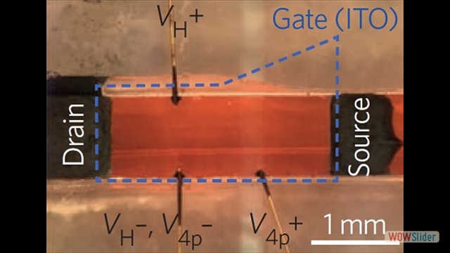
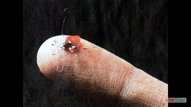
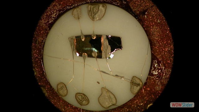
- Field-effect transistors (FETs) on novel nanomaterials.
- The fundamental photophysics of highly ordered organic semiconductors and perovskites (exciton dynamics, photoconductivity, light emission, and the photovoltaic effect).
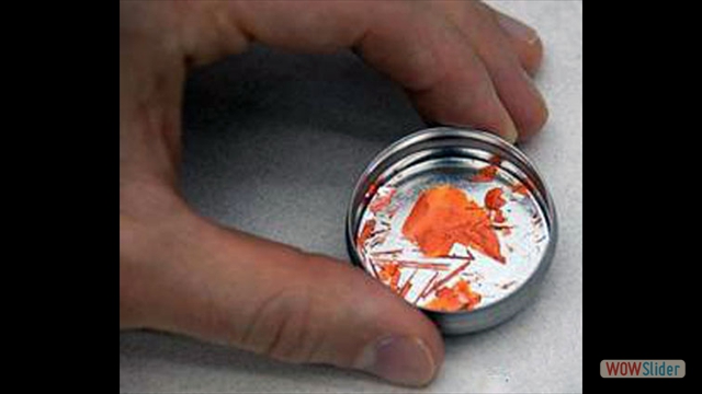
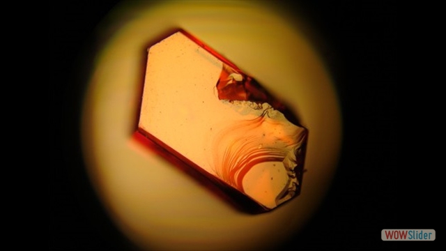
- Materials synthesis: growth of single-crystal organic semiconductors and epitaxial crystalline perovskites.
- Molecular self-assembly at functional interfaces.
- Layered inorganic semiconductors (dichalcogenides, graphene, 2D perovskites).
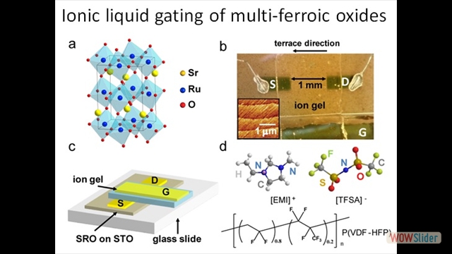
- Ionic-liquid gating of multiferroic oxides.
Watch video: High-resolution ac Hall effect measurements [video]
Watch video: Vacuum lamination approach to high-performance OFETs [video-1]
Watch video: Crystallization of TES-ADT on flexible substrates [video-2]
Fall MRS 2012, Tutorial Lecture: "Organic single crystals 101" [download file]
Latest News (click individual entry for abstract)
- Writing metallic nanostructures with focused ion beams. Electron. Mater. 2024
- Significant Joule self-heating pervasive in TFT literature. J. Mat. Chem. C. 2024
- Hall checklist: a practical guide for experimentalists. Nat. Electron. 2024
- Safe practices of mobility reporting discussed once again. Nat. Electron. 2024
- The 1st intrinsic (trap-free) perovskite FETs demonstrated. Adv. Mater. 2022
- Trully water-based (green) lithography suitable for delicate materials is demonstrated. Adv. Funct. Mater. 2021
- Emergence of n-type (electron) charge transport in heavily p-doped polymers is observed. Nature Mater. 2021
- Photo-Hall effect is measured for the 1st time in organic semiconductors. Adv. Funct. Mater. 2020
- Hall effect and Raman measured in rubrene as functions of strain. Adv. Sci. 2019
- Hall effect in polycrystalline OFETs is investigated. Adv. Funct. Mater. 2019
- PL gating effect is discovered in perovskites. Materials Today 2019
- Correlated flux scaling of PC and PL in perovskites. Phys. Rev. Applied 2018
- Artifact-free extraction of mobility in 4-probe FETs. Adv. Funct. Mater. 2018
- Critical assessement of mobility extraction in FETs. Nature Mater. 2018
- Polarization-dependent photoinduced bias-stress in OFETs. ACS Appl. Mater. & Interfaces. 2017
- Extended carrier lifetimes and diffusion revealed in hybrid perovskites by Hall effect. Nature Comm. 2016
- Intrinsic carrier mobility in hybrid perovskites is studied across phase transitions. Advanced Mater. 2016
- "Partial" carrier coherence in organic semiconductors is understood. Sci. Reports. 2016
- High-resolution ac-Hall effect methodology for OFETs is developed. Phys. Rev. Applied. 2016
- Multi-particle interactions and non-linear photoconductivity in rubrene. Sci. Reports. 2015
- Ionic-liquid gating of multi-ferroic oxide SrRuO3. Sci. Reports. 2014
- Trap healing and very high-resolution Hall effect in org. semiconductors. Nature Mater. 2013
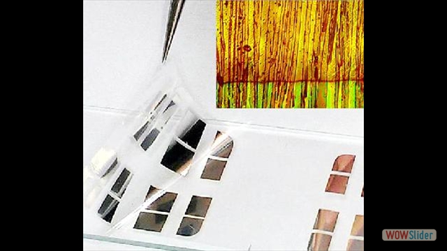
- Extremely flexible solution-processed organic devices are demonstrated. Nature Comm. 2012
- Dependence of nominal μ on VG sweep rate is revealed in disordered OFETs. PCCP 2012
- Bias stress effect is measured in "air-gap" OFETs. Advanced Mater. 2012
- Vacuum lamination approach to fabrication of high-performance OFETs. Advanced Mater. 2011
- The origin of PL spectral variability in crystalline organic semiconductors is revealed. Advanced Mater. 2011
- An amazing effect of photo-triggered diffusion of molecular oxygen in a crystalline organic semiconductor is reported. Advanced Mater. 2011
- The origin of the bias-stress instability in single-crystal OFETs is revealed. Phys. Rev. B 2010
- A very large exciton diffusion length (LEX ~ 3-8 μm) is observed in highly ordered organic semiconductors. Nature Mater. 2010
- D. J. Ellison from the group of Prof. Frisbie (University of Minnesota) has successfully applied Kelvin Probe Microscopy (KPM) to image SAM-rubrene system. Advanced Mater. 2010
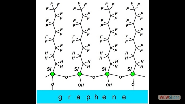
- A high-density hole-doped regime in graphene is realized by growing FTS SAM on top of the single-layer graphene FETs. Nano Lett. 2010
- Microscopic mechanism of SAM nucleation and growth on organic surfaces is revealed. Advanced Funct. Mater. 2009
- A molecular self-assembly of silanes on organic semiconductors is discovered. Nature Mater. 2008


 1
1 2
2 3
3 4
4 5
5 6
6 7
7 8
8 9
9 10
10 11
11 12
12 13
13 14
14 15
15 16
16 17
17 19
19 20
20